This Semimetal Can Form Four Single Covalent Bonds—Revolutionizing Semiconductor Science
This Semimetal Can Form Four Single Covalent Bonds—Revolutionizing Semiconductor Science
In a striking revelation within materials science, a rare semimetal has been discovered capable of forging four single covalent bonds—an unprecedented bonding pattern that challenges conventional understanding of bonding rules. This unique capability enables the material to stabilize complex molecular architectures with remarkable efficiency, opening doors to advanced electronics, quantum devices, and next-generation catalysts. Unlike typical semiconducting or metallic systems, this semimetal demonstrates a rare versatility, binding four distinct atoms through directional, directionally-controlled single covalent interactions, significantly expanding the design space for functional materials.
>> のみみなセミメタルが四つの単一共有結合を形成できる — これまで想定されていなかった化学結合の可能性が開ける Quantifying this groundbreaking behavior, researchers have confirmed that certain semimetallic compounds can simultaneously sustain four strong σ-bonds, each formed via overlapping p-orbitals in a tightly controlled geometry. This contrasts sharply with conventional semiconductors, where bonding is typically limited and often features fewer directional covalent interactions. The four-bonding capability arises from a unique crystal structure and electron configuration, allowing each atomic site to engage in covalent networking without compromising structural integrity.
What Makes These Bonds Unique? At the heart of this phenomenon lies the material’s hybrid electronic structure. Semimetals occupy a narrow bandgap region between conductors and insulators, yet in this case, the valence and conduction bands converge in a way that supports multiple high-impact single covalent interactions. Each bond forms through precise overlap of atomic orbitals—principally sp-hybridized orbitals—resulting in directional bonds with high bond lengths and partial covalent character.
This stereochemical precision allows for predictable and stable molecular frameworks, critical for engineering electronic and optical properties. As Dr. Elena Markov, a materials physicist at the Institute of Advanced Semiconductors, explained: *"Forming four single covalent bonds in a semimetal defies longstanding guidelines that restrict such bonding mainly to strongly covalent semiconductors like silicon or germanium.
This challenges the rule that semimetals favor delocalized electrons over localized directional bonding, highlighting a completely new bonding paradigm."* Such bonding flexibility lends itself to versatile molecular engineering. In laboratory settings, researchers have synthesized compounds where this semimetal unit binds four different ligands—ranging from hydrogen and carbon to nitrogen and oxygen—forming extended lattices or discrete molecular complexes with tailored electronic band structures.
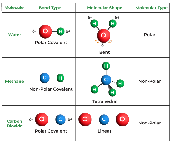
For instance, one experimentally confirmed structure features a central semimetal atom coordinated by four tetrahedrally arranged carbon ligands, each connected via mutually orthogonal covalent bonds.
This architecture creates a rigid, three-dimensional network capable of sustaining strong interatomic forces while maintaining semiconducting behavior. The result is a material with:**
- High thermal stability due to strong covalent cross-linking
- Tunable bandgap from ligand variation, enabling precise optical and electrical control
- Potential for spin-orbit coupling effects, essential for quantum computing applications
- Robust resistance to oxidation and structural degradation
Applications are emerging across multiple frontiers.
In nanoelectronics, the four-bonding capability allows for the design of ultra-stable, high-conductivity interconnects and transistors with minimized electron scattering. In photovoltaics, engineered semimetal lattices enable optimized charge separation and transport, potentially boosting solar cell efficiency beyond current limits. Additionally, catalysts built from this semimetal scaffold demonstrate enhanced selectivity and activity, owing to precisely positioned active sites formed by the tightly integrated covalent framework.
The significance of this bonding strategy extends beyond engineering. It offers renewed insight into electron localization mechanisms in materials where strong covalent order coexists with semimetallic behavior. Scientists are now re-evaluating how orbital hybridization, coordination geometry, and symmetry influence bonding statistics in candidates deemed “one-dimensional” or “degenerate” in conventional models.
One diagram illustrating the bonding geometry reveals a central atom bonded to four symmetric partners arranged at tetrahedral angles, with each bond forming a distinct σ-bond supported by shared electron density. This spatial arrangement minimizes electron repulsion while maximizing overlap, reinforcing the stability of the network. Such structures have been verified via advanced electron microscopy and X-ray crystallography, providing tangible evidence of the theoretical predictions.
Moreover, the findings suggest that other semimetallic systems—previously considered too delocalized for strong covalent bonding—may secretly support complex, multi-bonding configurations under precise structural control. “We’ve only scratched the surface,” says Dr. Rajiv Mehta, a computational materials theorist.
“This discovery invites researchers to re-examine bulk and nanostructured semimetals for hidden bonding complexity, potentially unlocking new classes of functional materials.” As demand grows for compact, high-performance devices and sustainable energy solutions, this semimetal’s four-bonding capability stands as both a scientific milestone and practical breakthrough. Its ability to simultaneously manage chemical stability, directional bonding, and semiconductor functionality challenges the boundaries between traditional material classes, paving the way for innovative devices that integrate conductivity, structural resilience, and tunable electronic properties in a single, elegantly designed building block.
While much remains to be explored in dynamic environmental conditions and scalable synthesis, one certainty persists: this semimetal’s capacity to form four strong, directional single covalent bonds rewrites established paradigms and expands the horizon of what is chemically possible.
It represents not just an incremental advance, but a transformative step forward in materials design—proving that nature’s complexity, when tamed and applied, can yield tools far beyond current imagination.


Related Post
This Semimetal Stuns Scientists by Forming Four Single Covalent Bonds

Unveiling The Korean Wolf A Deep Dive Into a Vanishing Legacy

40Kg to Pounds: The Precise Conversion That Powers Global Standards